


Seeing the unseen Synchrotron radiation opens up the nanoworld
Research on synchrotron light has enabled researchers to see and understand the structures and functions of nanoscale materials as never before. Among the leaders in this field is the University of Tokyo, which is employing the world’s brightest soft X-rays at its off-campus facility.
Nanolight Used to Observe Nano-World
The town of Sayo nestles snugly at the foot of a low-lying mountain range in Hyogo Prefecture, western Japan. High above the town is Harima Science Garden City, its skyline dominated by a huge silver-colored dome. The structure, 36 times the size of Koshien Stadium, one of Japan’s largest ballparks, is SPring-8, a synchrotron radiation facility managed by RIKEN and containing a powerful electron storage ring.

SPring-8: a world-class facility for synchrotron radiation science and analysis. The huge circle is the electron storage ring. © RIKEN
SPring-8’s electron storage ring generates highly brilliant, highly directional synchrotron radiation when the path of an electron beam, travelling at nearly the speed of light, is curved by a magnetic field.
In order to observe objects at the nanoscale, light with a wavelength shorter than the object under observation, and with sufficient focus to illuminate a small sample is required. SPring-8’s synchrotron light is mostly in the X-ray region of the spectrum, and consequently is suited to the observation of samples of nanoscale dimensions. Its energy is rated as the world’s highest. These capabilities are helping researchers to realize atomic-level analysis of structures and functions of sample objects, bringing about a wide array of scientific and industrial discoveries. Extending from the SPring-8 electron storage ring are 54 beamlines, each producing and guiding synchrotron light to their respective experimental stations. The long beamline, approximately 100 meters, runs into the University of Tokyo’s BL07LSU outstation, an off-campus facility, and is enabling researchers to conduct the world’s most advanced soft X-ray experiments.
The Search for Intense Brightness Started at the University of Tokyo
Scientists’ pursuit of synchrotron light for practical use dates back to the end of the 1960s, at which time the University of Tokyo’s Institute for Nuclear Study (Kakuken) produced synchrotron light in Japan. The accelerator ring was used for synchrotron radiation experiments when it wasn’t in use for its primary purpose of particle physics experiments. SOR-RING, the first dedicated electron synchrotron facility in the world, was built at Kakuken in 1974. SOR-RING was followed in 1981 by KEK-PF (Photon Factory), a part of the National Laboratory for High Energy Physics (KEK), now renamed the High Energy Accelerator Research Organization and a dedicated synchrotron radiation facility.[Edited 2012/11/29: see below.]

Eight undulators located in the University of Tokyo outstation. © Iwao Matsuda
Recalling those years, Professor Masaharu Oshima, director of the University of Tokyo’s Synchrotron Radiation Research Organization (SRRO), says, “KEK debuted just as the era of large accelerators was dawning, and many Kakuken members moved there en masse. You could say KEK inherited and continued their accelerator work.”
KEK-PF produced several leading-edge technology breakthroughs, among them the undulator. Synchrotron radiation had been generated by curving an electron path with a bending magnet, generating synchrotron radiation at each deflection. At KEK-PF, researchers found that using a regular array of magnets would cause an electron beam to “wiggle” or undulate in a periodical fashion, producing very bright and intense X-rays as a result of overlap or interference of the synchrotron radiation generated at the wiggle points. Many undulators were incorporated as the dominant light sources into SPring-8, completed in 1997, and enabled the facility to obtain the highest quality synchrotron radiation in the world.
Undulator technology has continued to improve. The University of Tokyo outstation, the world’s leading experimental environment for synchrotron radiation, now has eight of the most advanced undulators generating the world’s most intense beams of soft X-rays with variable polarization.
The University of Tokyo outstation has three fixed experimental stations. One of these employs a photoelectron spectrometer with a time resolution of 50 ps. By synchronizing laser and synchrotron light, this station can be used to observe changes over time as they are induced in samples such as photocatalysts. The second experimental station consists of a nano-beam photoelectron spectrometer with a spatial resolution of 70 nm, and is capable of observing three dimensional distribution of chemical-bonding states and electronic states. Soft X-rays are applied to a sample to examine its surface for two dimensions and the third dimension, depth, is obtained from the angle-resolved detection of photoelectrons. This approach is most suited for conducting structural analysis of electronic devices such as large-scale integrated circuits (LSIs). The third station is an ultrahigh-resolution emission spectrometer (energy resolution: 50 meV). Any sample, if radiated with synchrotron light, emits light of its own. For example, energy spectrum analysis of emitted light from proteins surrounded by water molecules and fuel cells generating electricity will reveal electronic states in their natural environment and during chemical reactions, respectively. Related experiments are being planned by SRRO’s Materials Science Division in a joint effort with SRRO’s Life Science Division.
“We’re focusing on these three experiments because of the need to investigate the actual states of new functional materials and devices vital to renewable energy sources in a ‘post-rare-metal’ era,” says Oshima, who is also a professor of the University of Tokyo’s Graduate School of Engineering. “If successful, we’ll obtain important additional knowledge and knowhow for energy and environmental sciences.”
Synchrotron Radiation Science Will Enable New Ways of Manufacturing
The University of Tokyo outstation came into use around November 2009. The excellent resolution of its measuring capability is highly regarded and the number of requests for its use has increased sharply, with the acceptance ratio now around 60%. With overseas requests also on the rise, competition for use of the facility is growing more acute by the year.

Schematic image of a three-dimensional photoelectron spectrometer, and Carbon 1s photoelectron intensity map of a graphene transistor where a P-region was detected at the Ni electrode-graphene interface.© Masaharu Oshima
This leading edge R&D facility has also helped foster a group of young researchers who will shape the future of synchrotron research. They have produced impressive results, among them successful research gains made in understanding fuel cell non-Pt carbon catalysts.
In addition, some members of the group recently solved the puzzle of why graphene transistors tend to show high resistivity. Graphene is a nanoscale carbon material. Scientists in Britain were awarded the Nobel Prize in Physics in 2010 for their trailblazing experiments on the material. Graphene features remarkably high electron mobility, operates at low voltage and consumes much less power than other materials, ideal properties for next-generation transistors.
Yet until recently, graphene transistor development had stalled, because when power is applied to the material, resistivity rises at the interface of the graphene film and metal electrodes, thus restricting electron mobility. Outstation members set about tackling this problem with the aid of their three-dimensional nano-beam photoelectron spectrometer. They found that a potential surge or upward band bending occurs at the metal-graphene interface at about 500nm — a phenomenon that shows the resistivity-increase results from N-type graphene turning into P-type graphene at the interface. While such nanoscale results had been predicted theoretically, this was the first time that such an interfacial band structure change has been observed. Oshima believes these discoveries by nano-beam photoelectron spectroscopy concerning exotic nanomaterials can also be applied effectively in creating new products.
“The development of new products from new materials used to require much experience and trial and error,” he stresses. “But the key is to utilize both synchrotron radiation and computational science to reveal the essential or intrinsic states of materials for new nano-materials with much higher performance and/or novel properties. Japan should embrace this approach to manufacturing as part of a new national strategy.” Synchrotron radiation is carving out a whole new world of manufacturing.
(Produced with cooperation of Scitech Communications)
[Edit: This article incorrectly stated that "SOR-RING was used for synchrotron radiation experiments when it wasn’t in use for its primary purpose of particle physics experiments" and that KEK-PF was Japan's first dedicated synchrotron facility. This has been corrected in the text. (Public Relations Division, 2012/11/29.)]
Researcher

Professor Masaharu Oshima
Graduate School of Engineering
Title image

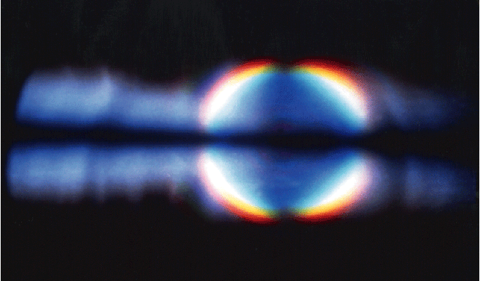
Brilliant synchrotron radiation emitted from undulator © The Institute for Solid State Physics & Synchrotron Radiation Research Organization