Atomic-scale characterization of electromagnetic structure in multiferroic materials Precise characterization of ferroelectric domain with sub-angstrom spatial resolution

The development of new materials for novel applications and devices requires advanced methods to accurately characterize their atomic and electromagnetic structures. In earlier research, Professor Yuichi Ikuhara’s group (Institute of Engineering Innovation, Graduate School of Engineering, the University of Tokyo) has developed a technique for directly observing the atomic structure of materials using the latest scanning transmission electron microscope (STEM). In addition, the research group has been working on a means of characterizing electromagnetic structures to a similar resolution.
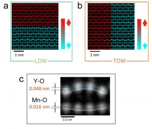
© Takao Matsumoto, Two types of ferroelectric domain walls. a: longitudinal domain wall (LDW), and b: transverse domain wall (TDW). Red color and blue color correspond to upward and downward polarization in the figure, respectively. Across both domain walls, atomically sharp transitions of polarization have been confirmed. c: An averaged high angle annular dark field scanning transmission electron microscope (HAADF-STEM) image of atomic structure obtained from a thin film of a hexagonal YMnO3 single crystal. The bright spot corresponds to the position of atomic column. Not only an evident atomic shift of 0.048 nm in Y-O layer, but also a tiny image shift of 0.016 nm in Mn-O layer is clearly revealed through a statistical image analysis.
In this latest research, an international team including Professor Yuichi Ikuhara, Associate Professor Naoya Shibata, and Senior Research Scientist Takao Matsumoto’s group at the University of Tokyo, collaborating with Dr. Hideo Kimura’s group at the National Institute for Materials Science, Tsukuba, Japan, and Professor Xiaolin Wang’s group at the University of Wollongong, Australia, employed a spherical aberration-corrected STEM and established a new technology to precisely characterize dielectric domain strength in multiferroic materials to sub-angstrom (less than 0.1nm) levels. This research, employing the latest electron microscope technology and statistical data analysis techniques, has made it possible to directly characterize not just materials’ atomic structure but also their electromagnetic structure at atomic resolution. This characterization technique is essential for the development of new piezoelectric materials in particular, and is expected to have a positive impact on their research and the search for materials for next-generation devices.
Research in Tokyo was conducted at the University of Tokyo’s Research Hub for Advanced Nano Characterization, supported by the Ministry of Education, Culture, Sports, Science and Technology (MEXT), Japan. Part of this work was conducted at the Green Network of Excellence (GRENE) and supported by “Nanotechnology Platform” (project No. 12024046), both sponsored by MEXT. This research was published online in Nano Letters on September 19, 2013 (GMT).
Paper
Takao Matsumoto, Ryo Ishikawa, Tetsuya Tohei, Hideo Kimura, Qiwen Yao, Hongyang Zhao, Xiaolin Wang, Dapeng Chen, Zhenxiang Cheng, Naoya Shibata, and Yuichi Ikuhara,
“Multivariate statistical characterization of charged and uncharged domain walls in multiferroic hexagonal YMnO3 single crystal visualized by a spherical aberration-corrected STEM”,
Nano Letters Online Edition: 2013/9/19 (GMT), doi: 10.1021/nl402158c.
Article link
Links
Graduate School of Engineering
Department of Materials Engineering, Graduate School of Engineering
The University of Tokyo Research Hub for Advanced Nano Characterization


