Demonstration of new ultra-low voltage tunneling transistors Zn-diffused junctions introduced into planar structures

The total power consumption of IT devices has shown a sharp rise in recent years, and is expected increase five-fold to account for 20% of total Japanese domestic energy consumption in 2025. As a result, limitation of supply voltage reduction of integrated circuits and increase in IT device energy consumption are currently important challenges.

© M. Noguchi, S. Kim, M. Yokoyama, O.Ichikawa, T. Osada, M. Hata, M. Takenaka, S. Takagi,
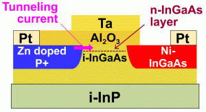
Cross sectional structure of field effect transistor (FET) using tunneling current, reported in this study. Here, InGaAs (Indium Gallium Arsenide) as the channel material, formed on InP (Indium Phosphide) substrates, has the p-type source region formed by Zinc (Zn) diffusion and the drain region composed of Nickel (Ni)-InGaAs alloy metal with Platinum (Pt) metal electrode contact. The MOS structure is composed of an Aluminum Oxide (Al2O3) gate insulator and Tantalum (Ta) gate electrode. Application of gate voltage makes the surface layer of InGaAs high-carrier concentration n-type, allowing to tunneling current in this surface region.
Professor Shinichi Takagi and Associate Professor Mitsuru Takenaka in the University of Tokyo Graduate School of Engineering Department of Electrical Engineering and Information Systems collaborating with Sumitomo Chemical Corporation have succeeded in development of a new transistor by using tunnel current able to operate using an extremely low supply voltage. In this study, the novel tunnel transistor with junctions composed of steep impurity profiles formed by Zn diffusion has been realized using almost the same device structure as in conventional MOS (metal-oxide-semiconductor) transistors. It has been demonstrated that this novel tunnel transistor exhibits world-record high ratio of on-current to off-current with steep current change on application of gate voltage.
This device is expected to provide a possibility to realize integrated circuits operating at supply voltage of 0.3 V and lower, leading to significant reduction in power consumption of IT devices as well as creation of new ultra-low power applications such as LSI (large-scale integration) devices without any batteries.
This study has been supported partially by the Japan Science and Technology Agency (JST) CREST Research Project “Innovative nano-electronics through interdisciplinary collaboration among material, device and system layers” (Development of Tunneling MOSFET Technologies for Integrated Circuits with Ultra-Low Power Consumption).
Paper
M. Noguchi, S. Kim, M. Yokoyama, O.Ichikawa, T. Osada, M. Hata, M. Takenaka, S. Takagi,
“High Ion/Ioff and Low Subthreshold Slope Planar-Type InGaAs Tunnel FETs with Zn-Diffused Source Junctions”,
2013 International Electron Device Meeting (IEDM)
Date: 2013/12/11
Links
Graduate School of Engineering
Department of Electrical Engineering and Information Systems (EEIS), Graduate School of Engineering


