New microscopy for the quantum world Direct imaging of local electric field at atomic dimensions

Ever since the invention of the microscope, the desire to observe the miniature world has been a driving force behind researchers’ efforts to understand the natural world, and even today that passion drives the development of improved microscopes.

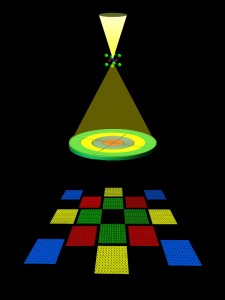
New detection system for electric field imaging © Naoya Shibata
When electrons pass through a material, they interact with the atoms in the material. This is measured by the annular detector (center) and an image of the material is built up (squares in the lower part of the image).
The electron microscope, an essential tool of modern science and technology which works by bombarding a target with electrons, has developed to the point where individual atoms can be observed. However, even though it is possible to observe atoms and the atomic structure of materials, it has proved extremely difficult to observe the localized electromagnetic fields around atoms. The technology to be able to do so has long been desired by materials science researchers.
University of Tokyo Graduate School of Engineering Associate Professor Naoya Shibata and Professor Yuichi Ikuhara and their research group, have succeeded in developing a special detector using a divided aberration-corrected scanning transmission electron microscope (STEM), and for the first time have succeeded in observing the interaction of an applied electron beam and localized electromagnetic field.
Using their technique, it is possible to observe the presence and intensity of electric fields on material surfaces or interfaces, a characteristic that affects the properties of the material. Applying this method to ferroelectric materials, it is possible to sensitively detect individual electric dipoles in unit cells within the material. It is hoped that the examination and comparison of atomic scale electromagnetic fields using this method will open up new approaches in research into materials for uses in many fields including in solar panels, fuel cells and batteries.
Press releasePaper
Naoya Shibata, Scott D. Findlay, Yuji Kohno, Hidetaka Sawada, Yukihito Kondo and Yuichi Ikuhara,
“Differential phase-contrast microscopy at atomic resolution”,
Nature Physics, Online Edition: 2012/6/24 (Japan time), doi: 10.1038/NPHYS2337.
Article link


