
ARTICLES

Electron microscope gains magnetic superpowers Researchers expand an electron microscope’s capacity to explore new domains
In a world first, a powerful transmission electron microscope (TEM) is given extraordinary new powers of sight, which allow it to view magnetic materials in unprecedented detail. The innovative upgrade modifies a key functional component of typical TEM design. This allows TEMs to probe magnetic samples, which ordinarily cannot be viewed by such devices. The upgrade opens up a broad range of research possibilities.
Every time a new invention to probe some part of reality is created, it expands our horizons. Around the turn of the 17th century, early microscopes gave us access to microorganisms and telescopes brought distant planets to the eyes of astronomers. Jump forward to the 20th century and electron microscopes eventually allowed people to view individual atoms. These devices have changed our world, but they have had one severe limitation — until now.
So what’s the issue with TEMs?
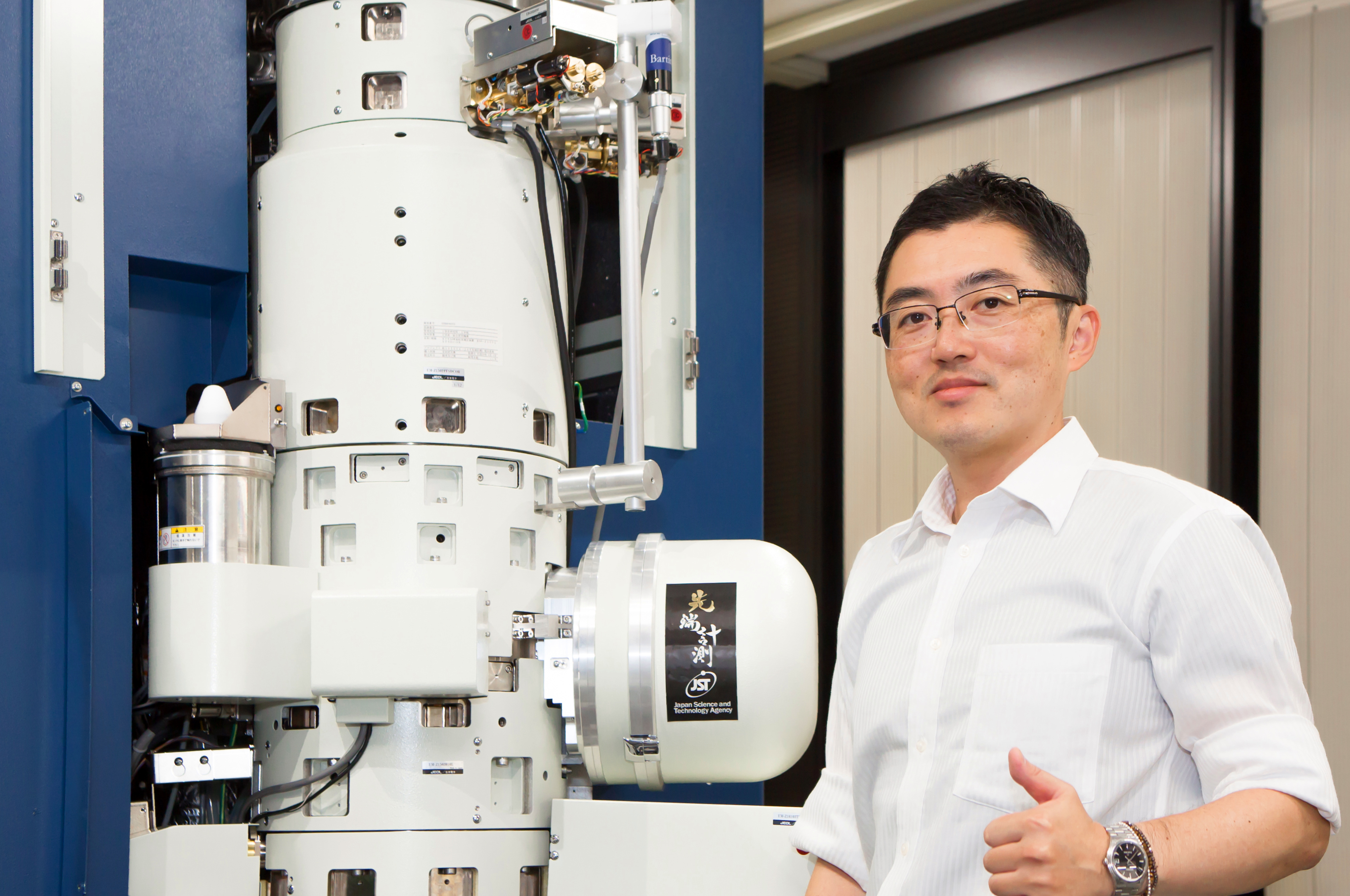
Professor Shibata with the unique upgraded TEM. Image: © 2019 Shibata et al.
TEMs work by firing a beam of electrons through a sample to create an image on a sensor behind the sample. A magnetic lens focuses the beam before it reaches the sample. This is analogous to the way an optical camera lens works. However, as the lens in a TEM is magnetic, it precludes the imaging of magnetic materials as both lens and sample would interfere with each other, ruining data and possibly even damaging expensive equipment.
This limitation is unfortunate as magnetic materials are not only interesting but are of crucial importance to much of modern society. Pretty much all electronic technology in some way makes use of magnetic materials. Frustrated, but not deterred, by this obstacle, Professor Naoya Shibata from the University of Tokyo’s Graduate School of Engineering and colleagues, in collaboration with JEOL Ltd., decided TEMs were due for an upgrade.
“I’ve spent years researching magnetic materials, including metals and ceramics,” said Shibata. “There are different microscopes that can view magnetic materials, such as scanning electron microscopes (SEMs), but unlike TEMs, those only view the outer surface of samples and with much lower resolution. The crux of the problem with TEMs is that the sample is placed inside the magnetic lens. So we explored ways to work around this and at long last, we’ve got it!”
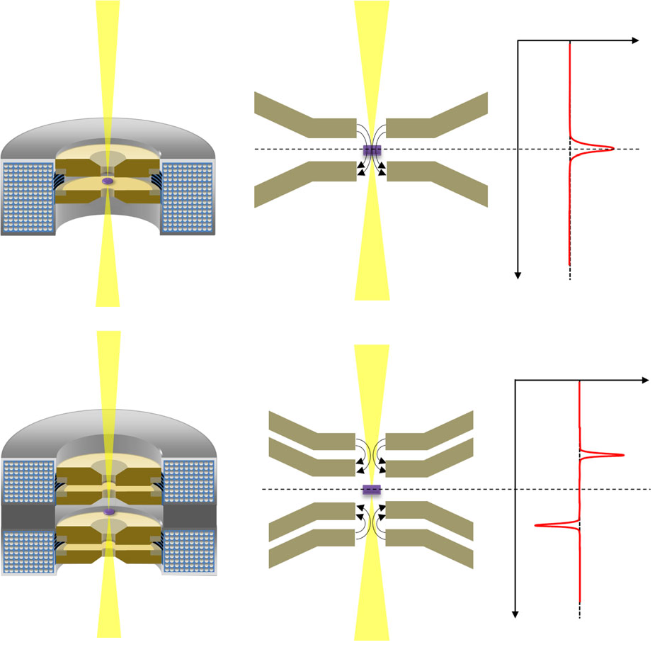
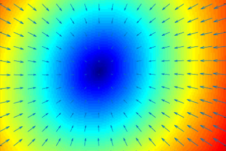
In the cutaway diagram of a typical TEM magnetic lens, The sample is at the heart of the magnetic field (top left). In a dual-lens system, the sample is placed between the lenses where the magnetic fields cancel out (bottom). Image: © 2019 Shibata et al.
How has the team solved the problem?
The solution is elegantly simple (at least in principle). Put some distance between the sample and lens; this keeps the sample magnetically isolated so the two components can’t magnetically interfere. This separation would ordinarily blur the resulting image, but Shibata and colleagues placed a second lens behind the sample, which brings the image back into focus.
Of course, the theory and especially the engineering are far more complex than that description, but that’s the basic idea. In reality, there is a large amount of image deformation or aberration that comes from using two lenses. However, in recent years, a lens aberration correction (LAC) system was invented, which the team incorporated into their upgrade.
LAC takes the form of another kind of magnetic lens that supplements the main ones. Jumping back to the camera lens analogy, were you to open one up you would see there are sometimes dozens of glass elements that make up the focusing system, each there to correct some aberration or other optical flaw with the primary lens. But there were issues besides magnetic field control that challenged the team.
“Once we had our dual-lens system and LAC in place, it was painful to still see a lot of noise in our test images,” continued Shibata. “One of the reasons for this was extraneous temperature change, magnetic fields and physical vibration from the external environment — cars, trains, that sort of thing. So we took great efforts to chill the lab without a noisy air conditioner. We also added active mechanical dampeners to cancel unwanted movement. And finally, it works.”
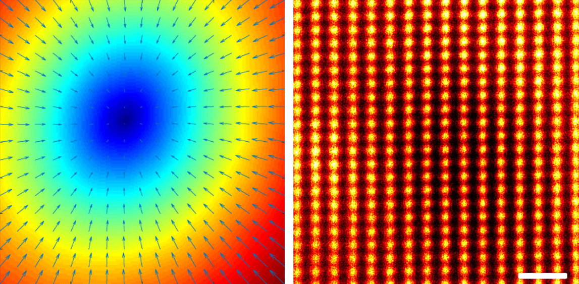
Experimental measurements of the magnetic field between the two lenses show the field is negligible in the center (left). A lattice of atoms in a magnetic iron compound, which was previously impossible to image (right). Image: © 2019 Shibata et al.
Now it exists, what can you do with it?
A TEM that can view magnetic materials opens up a whole new window on the world of materials science. Shibata can finally study metals and ceramics in detail, which could lead to the creation of new resilient materials. Physicists can study magnetism on the smallest scales to explore applications like ultrafast spintronic computers or high-capacity magnetic storage. And with a resolution of about one angstrom (one-ten billionth of a meter), Shibata hopes to directly view the magnetic field of an individual atom, which has never been seen before.
“Creating this delicate system and installing it into an electron microscope felt like we were performing heart surgery,” concluded Shibata. “But all the time and effort we’ve put into this is absolutely worth it to see the incredible images we can finally create. I hope to inspire new researchers in the field to explore what this technology can do and what it might lead to.”
Papers
N. Shibata, Y. Kohno, A. Nakamura, S. Morishita, T. Seki, A. Kumamoto, H. Sawada, T. Matsumoto, S.D. Findlay & Y. Ikuhara, "Atomic resolution electron microscopy in a magnetic field free environment," Nature Communications: May 24, 2019, doi:10.1038/s41467-019-10281-2 .
Link (Publication )
)