Strain enhances conversion efficiency from electrical to optical signal Toward low-power photonic integrated circuits using SiGe

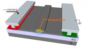
The research group of Associate Professor Mitsuru Takenaka in the University of Tokyo Graduate School of Engineering Department of Electrical Engineering and Information Systems, in collaboration with Sumitomo Chemical, Co., Ltd., has demonstrated for the first time that in a strained silicon germanium (SiGe) crystal, electrons and electron holes, which are positively charged as a result of the loss of an electron, induce an increased change in refractive index and absorption rates.
As a result, they have successfully developed low-power optical modulators capable of converting electrical signals into optical signals efficiently at the near-infrared wavelengths used for optical fiber communication. The newly-developed optical modulator can be fabricated in exiting semiconductor fabrication plants (fabs), enabling monolithic integration of low-power and large-scale photonic integrated circuits on electrical large-scale integrated circuits. This achievement is an important step towards realizing not only low-power and high-performance IT systems but also one-chip supercomputers with on-chip optical interconnections.This research was published in the online edition of the British journal Scientific Reports on Tuesday, 15 April 2014.
Paper
Y. Kim, M. Takenaka, T. Osada, M. Hata, and S. Takagi,
“Strain-induced enhancement of plasma dispersion effect and free-carrier absorption in SiGe optical modulators”,
Scientific Reports vol. 4, 4683, 2014, doi: 10.1038/srep04683.
Article link
Links
Graduate School of Engineering
Department of Electrical Engineering and Information Systems, Graduate School of Engineering


