
Physics and applications of semiconductor photonic nanostructures

- 1.3 Data Communication System (5G, Beyond 5G, IoT, Data Free Flow with Trust, etc.)
- 3.1 Data Processing Device/Material (Scaled CMOS, Novel Switch, 3D Integration, etc.)
- 3.3 Data Communication Device/Material (HF Device, IoT Device, etc.)
Satoshi Iwamoto
Research Center for Advanced Science and Technology
Institute of Industrial Science Professor
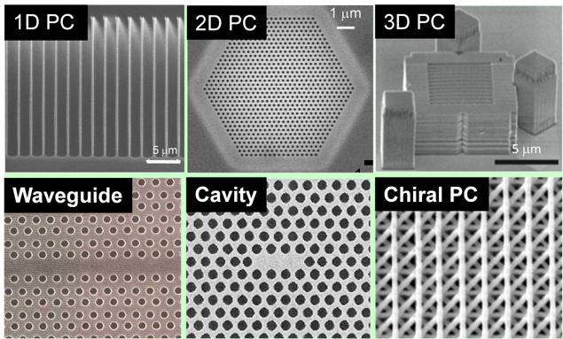
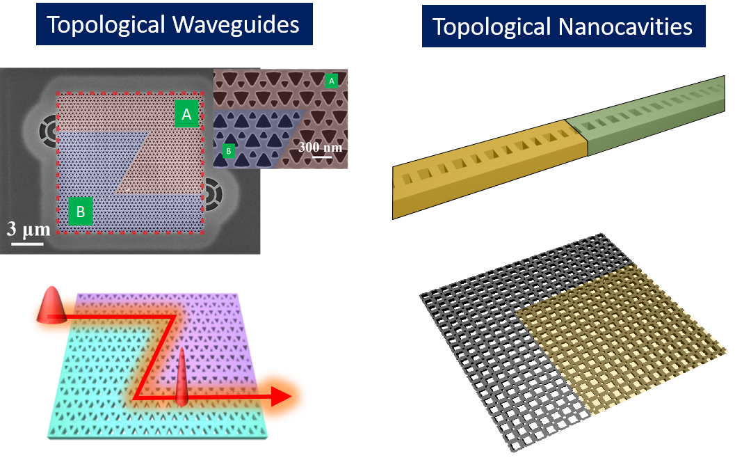
Miniaturization of photonics devices is highly demanded for future photonic integrated circuits. We are investigating semiconductor photonic nanostructures, such as photonic crystals, as a platform enabling the advanced control of the flow of light and light-matter interactions in a wavelength scale. We are also advancing research aimed at creating innovative nanophotonic devices that are utilizing the concept of topology.
The University of Tokyo
The University of Tokyo
Related links
Research collaborators
- Osaka University
- Tsukuba University
- Yokohama National University
- Tohoku University
- Kyoto Institute of Technology
- Kwansei Gakuin University
- Research Institute for Electromagnetic Materials
- University of Electro-Communications
- University of Twente
Related publications
- W.Lin, Y.Ota, Y.Arakawa and S.Iwamoto,"Microcavity-based generation of full Poincare beams with arbitrary skyrmion numbers", Phy. Rev. Research 3, 023055 (2021).
- H. Yoshimi, T. Yamaguchi, Y. Ota, Y. Arakawa, and S. Iwamoto, "Slow light waveguides in topological valley photonic crystals", Opt. Lett. 45, 2648 (2020).
- Y. Ota, F. Liu, R. Katsumi, K. Watanabe, K. Wakabayashi, Y. Arakawa, and S. Iwamoto, "Photonic crystal nanocavity based on a topological corner state", Optica 6, 786 (2019).
- Y. Ota, R. Katsumi, K. Watanabe, S. Iwamoto, and Y. Arakawa, "Topological photonic crystal nanocavity laser", Commun. Phys. 1, 86 (2018).
- T. Yamaguchi, Y. Ota, R. Katsumi, K. Watanabe, S. Ishida, A. Osada, Y Arakawa and S. Iwamoto, "GaAs valley photonic crystal waveguide with light-emitting InAs quantum dots", Appl. Phys. Express 12, 62005 (2019).