
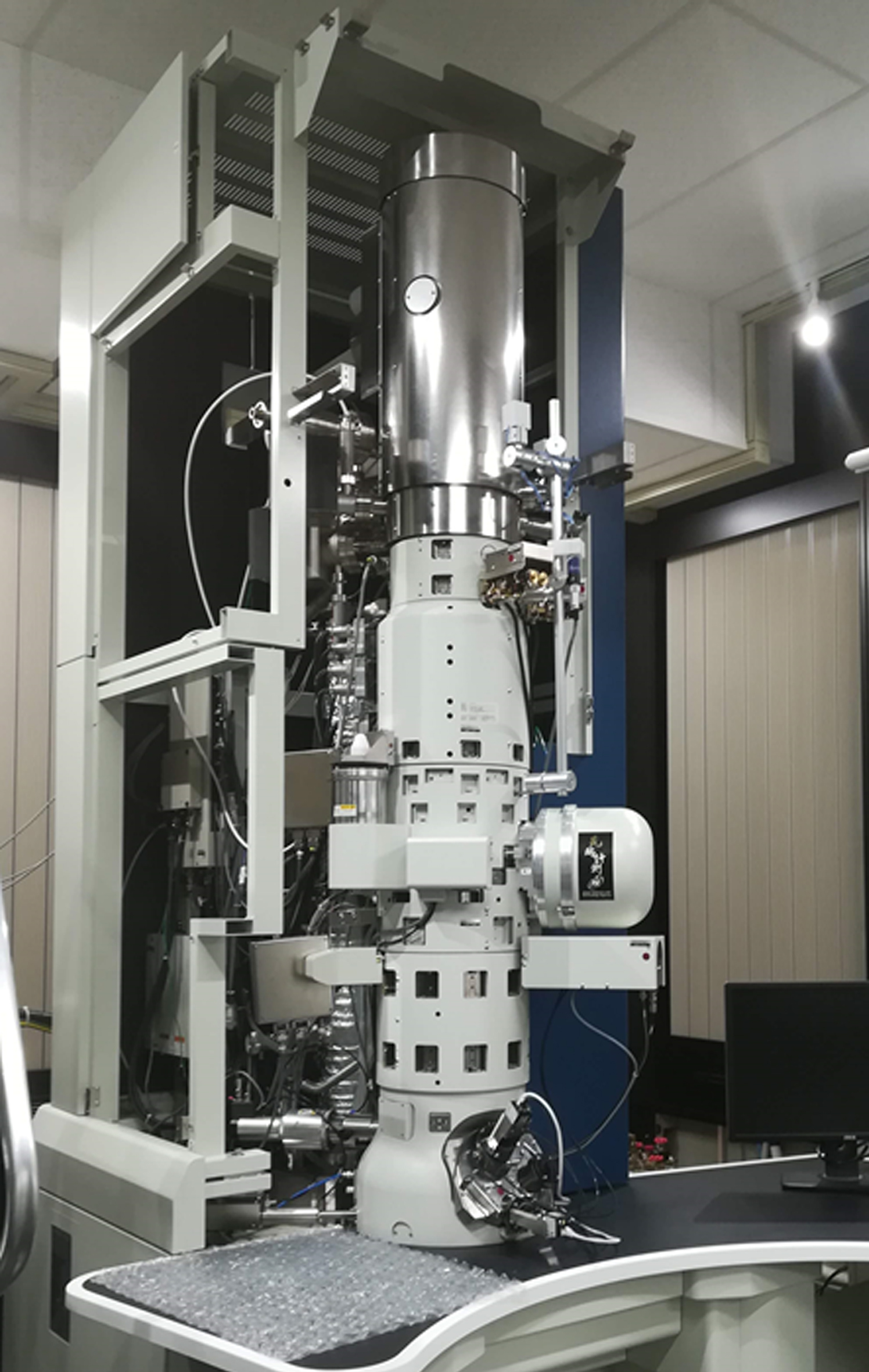
Development of an atomic-resolution magnetic-field-free electron microscope

- 2.1 Quantum bits, memories, devices(Superconducting circuits, Ion trapping, Trapped cold atoms, Photons, Quantum dots, etc.)
- 2.2 Quantum sensing(Quantum metrology/Sensing/Imaging, Optical lattice clocks)
- 2.3 Quantum materials(Topological materials/Thermoelectric devices/Functional materials)
- 2.5 Quantum wiring/Quantum electronics/Electronics for Quantum Information
Naoya Shibata
Graduate School of Engineering
Professor
We develop the first electron microscope that achieves atomic resolution in a magnetic-field-free environment, and apply this tool to local electromagnetic field analysis of quantum materials and devices.
Naoya Shibata

Naoya Shibata
Related links
Research collaborators
JEOL Ltd.
Related publications
N. Shibata et al., “Atomic resolution electron microscopy in a magnetic field free environment,” Nature Comm., 10, 2380 (2019).
N. Shibata et al., “Electric field imaging of single atoms,” Nature Comm. 8, 15631 (2017).
N. Shibata et al., "Differential phase-contrast microscopy at atomic resolution," Nature Physics, 8,611-615 (2012).
N. Shibata et al., “Electric field imaging of single atoms,” Nature Comm. 8, 15631 (2017).
N. Shibata et al., "Differential phase-contrast microscopy at atomic resolution," Nature Physics, 8,611-615 (2012).
Related patents
Transmission electron microscope US 8,431,897 B2 (2013.4.30)