
半導体フォトニックナノ構造技術とその応用

- 1.3 データ通信システム(5G・ポスト5G、IoT、DFFT など)
- 3.1 データ処理デバイス・マテリアル(微細CMOS、新原理スイッチ、3D集積 など)
- 3.3 データ通信デバイス・マテリアル(高周波デバイス、IoTデバイス など)
岩本 敏
先端科学技術研究センター
生産技術研究所 教授
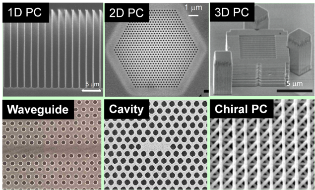
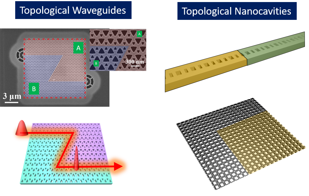
各種光デバイスの小型化・高機能化の実現を目指し、半導体フォトニック結晶などを用いた光および光と物質の相互作用の制御とその応用に関する研究を行っています。また、トポロジーの概念を活用した新機能ナノフォトニックデバイスの創出を目指した研究を推進しています。
東京大学
東京大学
プロジェクトに関するURL
共同実施者
- 大阪大学
- 筑波大学
- 横浜国立大学
- 東北大学
- 京都工芸繊維大学
- 関西学院大学
- 電磁材料研究所
- 電気通信大学
- Twente大学(オランダ)
主な関連論文
- W.Lin, Y.Ota, Y.Arakawa and S.Iwamoto,"Microcavity-based generation of full Poincare beams with arbitrary skyrmion numbers", Phy. Rev. Research 3, 023055 (2021).
- H. Yoshimi, T. Yamaguchi, Y. Ota, Y. Arakawa, and S. Iwamoto, "Slow light waveguides in topological valley photonic crystals", Opt. Lett. 45, 2648 (2020).
- Y. Ota, F. Liu, R. Katsumi, K. Watanabe, K. Wakabayashi, Y. Arakawa, and S. Iwamoto, "Photonic crystal nanocavity based on a topological corner state", Optica 6, 786 (2019).
- Y. Ota, R. Katsumi, K. Watanabe, S. Iwamoto, and Y. Arakawa, "Topological photonic crystal nanocavity laser", Commun. Phys. 1, 86 (2018).
- T. Yamaguchi, Y. Ota, R. Katsumi, K. Watanabe, S. Ishida, A. Osada, Y Arakawa and S. Iwamoto, "GaAs valley photonic crystal waveguide with light-emitting InAs quantum dots", Appl. Phys. Express 12, 62005 (2019).
関連するSDGs項目
- カテゴリナビ